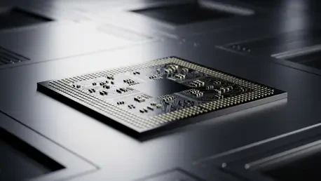

The rapid escalation of computational requirements for training large-scale generative models has forced the industry’s most prominent players to reconsider their foundational reliance on generic hardware architectures. Anthropic, recognized for its focus on safety, has entered into exploratory discussions with Samsung Electronics to design and manufacture its own proprietary silicon. This move signifies a shift toward vertical integration, as the company seeks to align its sophisticated algorithmic frameworks with hardware specifically tuned for its unique processing needs. By moving beyond off-the-shelf solutions, the developer aims to eliminate the latency and energy inefficiencies inherent in general-purpose graphics processing units. This potential partnership reflects a growing realization within the tech sector that the next frontier of artificial intelligence will not just be won through better code, but through the seamless marriage of software and dedicated physical circuitry.
Strategic Independence: Diversifying the Supply Chain
The primary catalyst for this hardware initiative is the imperative to mitigate the financial and logistical risks associated with the current market dominance of established chip manufacturers. For several years, the cost of acquiring high-end hardware has surged, often accounting for the majority of an AI firm’s operational expenditure. By engaging directly with a foundry like Samsung, Anthropic aims to secure a more predictable supply of chips while circumventing the intense bidding wars that occur for standard retail components. This strategy allows the firm to hedge against global supply chain disruptions that have previously slowed the deployment of large-scale clusters. Furthermore, custom-built silicon enables the enterprise to bypass the unnecessary features found in universal chips, focusing strictly on the matrix multiplications required for transformer-based models. This targeted approach promises to yield a significantly higher performance-per-watt ratio compared to traditional setups.
Beyond cost reduction, the move represents a fundamental desire for autonomy over the developmental roadmap of the hardware that powers the most advanced neural networks. Currently, AI researchers must wait for external vendors to release new architectures before they can implement certain software optimizations. By designing its own application-specific integrated circuits, the organization can influence the very architecture of the chip to support future iterations of its Claude model family. This proactive stance ensures that the hardware does not become a limiting factor as researchers experiment with novel architectural layers or sparse attention mechanisms. Moreover, having a direct relationship with a semiconductor manufacturer provides deeper visibility into the production cycle, allowing for better long-term capacity planning. This level of control is increasingly seen as a prerequisite for any company aspiring to lead the market in high-performance computing and complex model inference.
Technical Synergy: Balancing Custom Silicon with Global Infrastructure
Samsung presents a compelling technical advantage due to its advanced manufacturing nodes, particularly its expertise in the gate-all-around transistor architecture. As the industry transitions to the 2-nanometer process, this technology becomes crucial for managing the heat and power consumption of massive data centers. Unlike traditional designs, this specific architecture allows for better current control, which directly translates to faster switching speeds and lower leakage. For a developer like Anthropic, these improvements are not merely incremental; they are essential for scaling inference capabilities without exponentially increasing electricity costs. Additionally, Samsung’s unique position as both a foundry and a premier provider of high bandwidth memory offers an integrated solution that few other partners can match. The tight coupling of logic and memory is vital for reducing the “memory wall” bottleneck, where data transfer speeds often limit the overall efficiency of AI systems.
The exploration of custom hardware by leading AI laboratories established a clear roadmap for the future of specialized computing environments. This evolution required a meticulous focus on forging deep technical alliances with foundries and recruiting specialized talent to oversee the transition from software to silicon. To remain competitive, organizations found it necessary to evaluate their specific workloads and determine where custom ASICs could provide the most significant energy and cost savings. Future considerations for the industry included the expansion of regional manufacturing capabilities and the development of standardized interconnects to ensure that custom chips remained compatible with global cloud standards. Leaders in the field moved toward securing long-term wafer supply agreements and investing in design tools that shortened the cycle from concept to production. These steps ensured that hardware was no longer a static utility but a dynamic component that actively contributed to the safety of AI models.