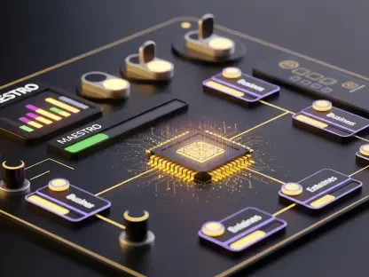

Laurent Giraid, a technologist whose work lies at the intersection of artificial intelligence and semiconductor engineering, joins us to demystify a groundbreaking development in analog chip design. For decades, this critical process has been a bottleneck, relying on the intuition and experience of senior engineers rather than automation. We’ll explore how new AI techniques are overcoming the persistent challenge of data scarcity by learning to generate their own training material. Giraid will explain the power of a unified “foundation model” capable of handling multiple design tasks, the intricate process of teaching an AI to recognize and replicate complex circuit patterns, and the remarkable accuracy it has achieved. Finally, we’ll look ahead at what it will take for this technology to transition from the research lab to the production floor.
Data scarcity has historically constrained AI adoption in analog design. How does your self-supervised method of masking and predicting layout patches generate useful training data? Could you share some metrics on how this reduces data dependency compared to conventional approaches?
This is really the heart of the problem we set out to solve. Analog layout data is a closely guarded secret, the “crown jewels” of any semiconductor firm, which makes training a data-hungry AI nearly impossible. So, instead of waiting for a massive, public dataset that will never appear, we taught the model to create its own curriculum. We take existing, albeit limited, layout designs and break them down into small, digestible patches. Then, we play a sort of “peek-a-boo” with the AI—we digitally cover up, or mask, a part of the patch and challenge the model to predict exactly what’s missing. By repeating this process millions of times, the AI starts to internalize the fundamental rules and relationships of analog design without any human labeling. From just six real layout datasets, we were able to generate about 320,000 unique training samples. The results are striking: our model achieved performance comparable to traditional AI methods while using only one-eighth of the data they would typically require. It’s a massive leap in efficiency.
Your research highlights using a single foundation model for diverse tasks like metal routing and N-well generation. What are the primary advantages of this unified approach over building separate AI models for each task? Please describe the process of adapting the pre-trained model for a new function.
The biggest advantage is efficiency, both in terms of development time and computational resources. Building, training, and maintaining a separate, specialized AI for every single task—contact generation, via generation, metal routing, and so on—is an immense undertaking. It’s like hiring a different specialist for every minor step on an assembly line. Our foundation model approach is more like training a highly skilled, versatile engineer. We first conduct a broad “pre-training” phase where the model learns the universal language of analog circuits—the recurring structures and common patterns that appear everywhere. Once it has this solid, foundational knowledge, adapting it to a new, specific task is remarkably straightforward. We only need a small amount of task-specific data to fine-tune it. This not only dramatically reduces the overall design workload but also ensures a consistent design philosophy across all stages, which is a subtle but powerful benefit.
Achieving a 96.6% success rate in passing both design-rule and schematic verification is a significant benchmark. What were the key challenges in reaching this level of accuracy, and can you provide an example of a layout solution the model produced that was particularly efficient or innovative?
Reaching that 96.6% success rate was a grueling but rewarding process. The main challenge wasn’t just teaching the AI to place components, but to do so while respecting an enormous web of intricate design rules and ensuring the final layout perfectly matched the original schematic. These rules can be contradictory, and a tiny violation can render the entire chip useless. It’s a classic needle-in-a-haystack problem. The breakthrough came when the model started demonstrating an almost intuitive understanding of layout optimization. For instance, in one of the metal routing tasks, the model produced a solution that used a more compact and direct path than a junior engineer might have attempted. It cleverly navigated around other components in a way that minimized signal interference and parasitic capacitance, not because it was explicitly told to, but because its pre-training on thousands of examples had taught it that this type of pattern leads to a successful, robust design. It was a clear sign the AI was not just mimicking, but genuinely learning the craft of layout design.
The model was pre-trained to recognize recurring structures common in analog circuits. What specific kinds of patterns does the AI learn to identify, and how does this foundational knowledge enable it to generate layouts that are both functional and compliant with complex design rules?
During the pre-training, the AI essentially develops an eye for the fundamental building blocks of analog design. It learns to identify things like differential pairs, which need to be perfectly symmetrical for optimal performance, or current mirrors, where transistors must be matched with extreme precision. It also recognizes common placement strategies, like how sensitive components are shielded from noisy digital logic or how dummy patterns are inserted at the edges of a design to ensure manufacturing consistency. This foundational knowledge acts as a set of learned instincts. So, when the model is later tasked with a specific job like N-well generation, it doesn’t start from a blank slate. It already understands, for example, that certain transistors need to be enclosed within that well and that the well must maintain specific distances from other features. This inherent understanding allows it to generate layouts that are not only compliant by the book but are also robust and well-crafted from an engineering perspective.
You mentioned the goal is to develop this technology to a “practically usable level.” What specific performance benchmarks must be met for this AI to be integrated into the workflows of semiconductor firms, and what are the next steps for gathering data and enhancing the model?
Moving from a research success to a “practically usable level” means meeting the industry’s uncompromising standards for speed, reliability, and quality. First, we need to push that 96.6% success rate even closer to 100%, because in chip manufacturing, anything less than perfect is a failure. Second, the AI must be fast—it needs to generate these layouts in a fraction of the time a human team would take. And third, the quality of its output must consistently rival that of an experienced engineer. Our next steps are twofold. We need to expand our dataset significantly; the more high-quality layouts the model sees, the more robust and intelligent it will become. We’re actively looking to collaborate and acquire more data to continue this large-scale learning. Concurrently, we are refining the model’s architecture to better handle even more complex and varied circuit designs, pushing its capabilities until it becomes an indispensable tool in every analog designer’s toolkit.
What is your forecast for AI in analog semiconductor design?
I believe we are at a pivotal moment. For the next five to ten years, AI will not replace human designers but will evolve into an incredibly powerful collaborator. We’ll see foundation models like this integrated directly into design software, acting as an expert assistant that can instantly generate multiple high-quality layout options for an engineer to review and refine. This will eliminate the most tedious and time-consuming aspects of the job, freeing up engineers to focus on higher-level system architecture and innovation. AI will handle the painstaking rule-checking and routing, allowing for a level of design exploration that is simply impossible today. In the longer term, as these models become more sophisticated, they will begin to automate the entire analog layout process for a wider range of circuits, dramatically shortening the chip development cycle from years to months and fueling the next wave of technological advancement.