
The silent architecture of the modern technological landscape depends entirely on invisible imperfections that define the very limits of physical endurance and electronic capability, where a single misplaced atom can either ruin a processor or double its efficiency. Within the corridors of advanced material science, the traditional view of a defect as a simple structural failure has shifted toward a more sophisticated understanding of imperfections as essential engineering tools. These atomic irregularities are no longer seen as mere accidents of manufacturing but as intentional modifications that dictate how a material interacts with light, electricity, and mechanical stress.
The strategic implementation of these useful flaws remains a cornerstone in the development of next-generation semiconductors and high-strength alloys. In the automotive and aerospace industries, for instance, controlling the distribution of carbon and other elements within a steel lattice is what provides the necessary integrity for critical safety components. Similarly, in the renewable energy sector, the efficiency of solar cells depends heavily on the precise management of impurities that facilitate electron movement. Despite these advancements, the industry has long struggled with the limitations of characterization techniques that often damage the very samples they aim to analyze.
The current trajectory of the industry indicates a significant shift toward data-driven manufacturing processes that minimize the reliance on trial-and-error methodologies. As we progress through 2026, the growing influence of artificial intelligence in crystal lattice manipulation is becoming the primary driver of innovation. By moving away from qualitative observations toward quantitative, predictive modeling, researchers are finally beginning to master the atomic landscape with a level of control that was previously relegated to theoretical physics.
Advancing Diagnostic Precision Through Machine Learning
Emerging Trends in Non-Invasive Atomic Characterization
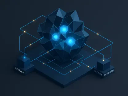
The evolution of materials science is currently defined by a transition from basic observation to high-fidelity, AI-driven analysis. Researchers at the Massachusetts Institute of Technology have recently introduced a groundbreaking approach that utilizes foundational models to interpret complex crystallographic data. This method relies on the integration of multihead attention mechanisms, which are designed to process massive datasets by identifying specific patterns within a noise-heavy environment. This technology allows engineers to move beyond the era of blind doping, where impurities were added to semiconductors based on probabilistic outcomes rather than verified placement.
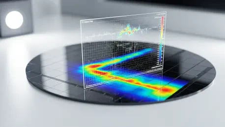
The core of this advancement lies in the refinement of vibrational spectroscopy as a signature-based diagnostic tool. Every material possesses a unique atomic vibration, or phonon spectrum, which changes when a defect is introduced. In the past, interpreting these shifts was a monumental task because different types of defects often produced overlapping signals that were indistinguishable to human analysts. However, the application of machine learning models allows for the isolation of these signatures, enabling the identification of specific atomic-scale disruptions without the need for invasive or destructive procedures.
Moreover, this shift toward non-invasive diagnostics facilitates a more integrated approach to material fabrication. By using foundational models trained on thousands of known crystal structures, the AI can predict how a specific dopant will affect the overall stability and performance of a material before a single gram is synthesized. This predictive capability is transforming the role of the materials engineer from an experimentalist into a digital architect who can simulate and verify complex lattice configurations in a virtual environment.
Market Projections and the Performance Metrics of AI Integration
The economic landscape of the global semiconductor and high-performance alloy markets is undergoing a rapid transformation as precision engineering becomes the standard. From 2026 to 2030, the adoption of AI-driven characterization tools is expected to accelerate, driven by the need for higher yields in microelectronics and more durable materials for energy storage. Statistical performance metrics from the MIT model indicate that it can detect up to six simultaneous point defects with a sensitivity level of 0.2 percent. This degree of precision provides a significant competitive advantage for manufacturers who require extreme material purity.
The reduction in material waste and research and development cycles is another critical factor influencing market growth. By utilizing predictive defect modeling, companies can avoid the costly production of batches that fail to meet specifications. In contrast to older methods that required destructive sampling, the new AI-integrated workflows allow for holistic quality control across the entire production line. This transition is not only an engineering milestone but an economic one, as it lowers the barrier to entry for the development of exotic materials that were once considered too difficult to characterize reliably.
Industry forecasts suggest that the integration of these technologies will lead to a more resilient supply chain for critical components. As manufacturers move toward automated, real-time diagnostic systems, the time between a material’s conceptualization and its market debut will shrink significantly. This efficiency is particularly vital for the battery technology sector, where the quest for higher energy density requires a near-perfect understanding of atomic-level interactions during charge and discharge cycles.
Overcoming the “Blind Men and the Elephant” Diagnostic Dilemma
The primary obstacle in material characterization has historically been the fragmentation of existing techniques, where different methods provide only partial views of the internal structure. Tools like X-ray diffraction and transmission electron microscopy are powerful, but they often struggle to reconcile their findings into a single, cohesive picture of a material’s health. This diagnostic dilemma has frequently left engineers in a position where they can see that a material is failing but cannot precisely identify which combination of impurities or structural shifts is responsible for the decline in performance.
Technical hurdles in resolving overlapping signals from multiple impurities have plagued the industry for decades. When several types of defects coexist, their vibrational signatures merge into a complex wave that traditional analysis cannot easily unravel. The MIT researchers addressed this by developing strategies to reconcile experimental neutron-scattering data with vast computational databases. This allows the AI to serve as a bridge, connecting the high-resolution but destructive images provided by microscopy with the broader, low-resolution data obtained from non-invasive scans.
This synthesis of data sources effectively ends the fragmentation of diagnostic information. By creating a unified model that can interpret signals from various spectroscopic sources, the industry is moving toward a standard where a single scan can reveal the complete state of a material. This capability is essential for high-stakes applications where the presence of even a minor, unidentified impurity could lead to catastrophic structural failure or electronic malfunction.
Standardizing Quality Control and Compliance in Advanced Manufacturing
The introduction of AI into the laboratory is also playing a pivotal role in establishing a new ground truth for material certification and industry standards. In sectors like aerospace and microelectronics, where safety and reliability are paramount, regulatory compliance requires a rigorous level of documentation regarding material purity. The ability to quantify defects with statistical certainty provides a verifiable record that can be used to meet these strict requirements. This standardization is critical for the global trade of high-tech components, ensuring that a material produced in one region meets the exact specifications required in another.
Security and reliability implications are equally significant when considering the critical infrastructure components that power modern cities. Unintended defects in large-scale power transformers or structural beams can remain hidden for years until they fail under stress. AI-driven monitoring provides a way to identify these vulnerabilities during the manufacturing phase, long before they are deployed in the field. By developing universal benchmarks for defect concentration, the industry can create a more transparent and secure foundation for the technology that society relies upon daily.
The transition toward these standards is likely to be supported by new regulatory frameworks that mandate the use of high-precision characterization for critical infrastructure. As the technology becomes more accessible, the expectation for material transparency will grow, pushing manufacturers to adopt more sophisticated AI tools. This shift will ensure that the quality of materials is no longer a matter of probability but a matter of verifiable scientific fact.
The Future of Defect Engineering and Scalable Innovation
As the industry moves forward, the expansion of AI diagnostics is expected to transition from specialized facilities to more accessible laboratory settings. While neutron scattering remains a gold standard for research, the team at MIT is working toward scaling these models for use with Raman spectroscopy. This change will democratize access to high-precision defect analysis, allowing smaller manufacturers and research institutions to benefit from the same level of atomic insight that was once reserved for national laboratories.
Future-proofing materials will also involve scaling these models to identify more complex structural issues such as dislocations and grain boundaries. While point defects are relatively simple to model, the interactions between different types of structural shifts are much more complicated. The next generation of AI tools will likely possess the capability to map these interactions in three dimensions, providing a real-time, in-line defect monitoring system for smart factories. This would allow for the immediate adjustment of manufacturing parameters the moment a deviation is detected, ensuring that every product off the line is virtually perfect.
The impact of global economic shifts will further accelerate the adoption of these high-precision technologies. As the cost of raw materials fluctuates and the demand for energy-efficient electronics rises, the ability to do more with less becomes a primary survival strategy for tech firms. Precision defect engineering allows for the creation of thinner, lighter, and more powerful components, ensuring that innovation can continue even in the face of resource constraints.
Redefining the Paradigm of Material Reliability and Investment
The breakthrough achieved by the researchers at MIT effectively transformed the process of material characterization from a series of high-stakes guessing games into a precise and quantifiable science. By applying advanced machine learning to the nuances of atomic vibrations, they provided a pathway to understand the secret life of crystals. The results of their study demonstrated that AI could not only identify the presence of flaws but also measure their exact impact on a material’s functional properties.
The long-term value of mastering the double-edged sword of atomic imperfections was proven through the increased efficiency and reliability of the materials tested. This success signaled to stakeholders in battery technology, electronics, and renewable energy that the future of their industries lies in the marriage of AI-driven diagnostics and manufacturing excellence. The strategic recommendations stemming from this shift emphasized the need for continued investment in non-invasive characterization tools that can keep pace with the increasing complexity of modern devices.
Ultimately, the paradigm of material reliability was rewritten to include a far more granular level of scrutiny. The industry moved toward a future where the unpredictability of physical substances was mitigated by the clarity of digital models. This evolution ensured that the materials forming the backbone of the next technological age were stronger, smarter, and more reliable than anything that had come before. Strategies for material development became more focused on the deliberate management of flaws, turning every imperfection into a calculated advantage.