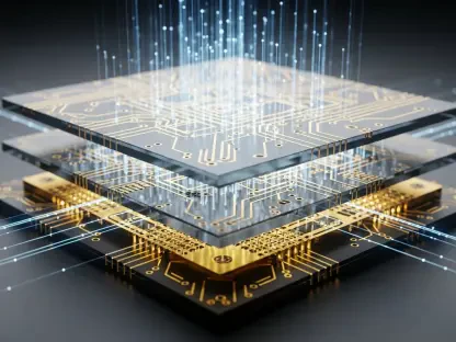

AI inference systems are on the brink of a major transformation with the development of WaferLLM, a breakthrough in wafer-scale computing introduced by researchers from the University of Edinburgh and Microsoft. By integrating hundreds of thousands of cores onto a single chip, WaferLLM promises to revolutionize AI hardware with unparalleled computational power and energy efficiency.
Revolutionizing AI Hardware
Unmatched Computational Power
WaferLLM’s innovative design allows it to handle large-scale AI tasks with superior performance. Unlike traditional GPU-based systems, WaferLLM combines multiple dies onto a single wafer, creating a powerful computing platform that can process complex computations with ease. This integration results in an unprecedented computational capability that can significantly boost the performance of AI inference tasks. The high-density integration of cores onto a single chip not only enhances processing speed but also reduces latency, ensuring swift data handling for demanding applications.
The architecture of WaferLLM leverages wafer-scale technology to achieve this high level of integration. By utilizing advanced fabrication techniques, the system minimizes the physical distance between cores, reducing communication delays and enabling faster computation. This approach is especially beneficial for handling the vast amounts of data and intricate calculations required by large language models (LLMs). With the ability to execute numerous operations simultaneously, WaferLLM offers a substantial uplift in performance, making it a game-changer in the field of AI hardware.
Surpassing GPU Limitations
Current AI systems rely heavily on GPUs, which face challenges in scalability and efficiency. WaferLLM employs advanced parallel computing strategies, overcoming these obstacles and providing a more effective solution for large language models. GPUs, while powerful, have intrinsic limitations when it comes to scaling up for extreme levels of parallel processing. They are designed to perform well under specific workloads, but their efficiency drops when spreading across multiple chips or when tasked with exceptionally large models.
WaferLLM mitigates these limitations through its wafer-scale approach, which centralizes computational resources. This design minimizes the need for inter-chip communication, a common bottleneck in traditional GPU setups. By maintaining all processing units on a single substrate, WaferLLM ensures that data transfers are both rapid and efficient, leading to better overall system performance. This architectural shift is critical for the next generation of AI applications, which demand increasingly higher levels of computational power and efficiency.
Energy Efficiency Breakthrough
Superior Sustainability
One of the standout features of WaferLLM is its remarkable energy efficiency. It achieves 22 times greater energy efficiency compared to advanced GPUs, making it a sustainable choice for AI inference, particularly in energy-hungry data centers. This leap in efficiency is achieved through a combination of optimized power distribution and reduced overhead associated with inter-chip communications. The single-wafer design of WaferLLM eliminates the need for energy-intensive data transfer between chips, contributing to its lower power consumption.
WaferLLM’s energy efficiency addresses a crucial concern in the AI industry: the environmental impact of data centers. As AI models grow in complexity and size, the computational demands—and thus energy consumption—have skyrocketed. WaferLLM’s design offers a path to mitigating this problem by providing high-performance AI inference with significantly lower energy requirements. This contributes not only to reduced operational costs for data centers but also to broader sustainability goals, aligning with global efforts to minimize environmental footprints.
Reduced Power Consumption
By minimizing power consumption without sacrificing performance, WaferLLM marks a significant step toward creating environmentally friendly AI systems. This efficiency not only reduces operational costs but also aligns with global goals for energy sustainability. WaferLLM achieves this by utilizing energy-saving techniques such as dynamic voltage and frequency scaling (DVFS), which adjust power use based on workload demands. This ensures that the system operates in the most energy-efficient mode possible at all times.
The reduction in power consumption also translates to lower heat generation, reducing the need for extensive cooling infrastructure in data centers. This dual benefit of lower energy use and reduced cooling requirements further amplifies the cost savings and environmental benefits of adopting WaferLLM. As the AI industry continues to expand, the demand for sustainable and energy-efficient solutions becomes ever more critical. WaferLLM sets a new standard in this regard, offering a compelling combination of performance and sustainability that other AI hardware solutions will strive to match.
Future Impact and Applications
Shaping AI’s Future
WaferLLM’s principles extend beyond AI inference. Its scalable architecture has the potential to impact real-time analytics, scientific simulations, and edge computing, potentially transforming various technological fields. The inherent flexibility and advanced capabilities of WaferLLM make it suitable for a wide range of applications that benefit from high-speed data processing and efficient computation. Real-time analytics, for example, can leverage WaferLLM’s fast processing power to analyze vast datasets on the fly, enabling quicker decision-making in industries such as finance, healthcare, and logistics.
In scientific simulations, WaferLLM’s powerful computational resources can handle complex mathematical models and large-scale simulations with greater accuracy and speed. This can accelerate research and innovation in fields like climate science, physics, and biomedical engineering. Furthermore, edge computing applications can benefit from WaferLLM’s energy efficiency and compact form factor. Deploying WaferLLM at the edge allows for advanced AI capabilities close to the source of data generation, reducing latency and enhancing real-time processing in IoT devices, autonomous vehicles, and smart cities.
Advancing AI Models
With the ability to maintain performance improvements as more compute units are added, WaferLLM is well-suited to manage increasingly complex AI models. This capability is essential for integrated multi-modal learning systems and other advanced AI applications. As AI models grow more sophisticated, the demand for computing power doubles. WaferLLM’s scalable nature ensures that as these models expand, the system can accommodate additional computational load without performance degradation.
The architecture of WaferLLM supports the incremental addition of compute units, allowing it to adapt to the needs of evolving AI technology. This is particularly beneficial for research and development environments where AI models are continuously being upgraded and refined. Integrated multi-modal learning systems, which require the fusion of various data sources and types, particularly benefit from WaferLLM’s high bandwidth and low latency, enabling seamless data integration and processing. This capability enhances the potential for breakthroughs in areas like natural language processing, computer vision, and autonomous systems.
Overcoming Challenges
Data Communication Solutions
Efficient data communication across numerous cores is crucial for wafer-scale systems. WaferLLM addresses this with decentralized data handling strategies, reducing bottlenecks and enhancing overall system performance. The complexity of managing data flow in a densely packed wafer requires innovative solutions to ensure that information is transmitted accurately and swiftly between cores. WaferLLM implements a decentralized approach to data handling, distributing the data processing tasks across multiple cores to prevent any single point of failure.
This method not only improves reliability but also optimizes data transfer rates by localizing communication paths. The decentralization ensures that cores can operate independently of a central control unit, significantly reducing the risk of bottlenecks that could hamper performance. This is essential for maintaining the high efficiency and speed that wafer-scale computing promises. Additionally, WaferLLM’s architecture includes advanced error correction and fault detection mechanisms to ensure that data integrity is preserved during transmission, further boosting the robustness of the system.
Addressing Manufacturing Complexities
Despite its advantages, wafer-scale computing comes with significant manufacturing challenges. The complexity of integrating multiple dies onto a single wafer can affect production costs and yield rates, posing obstacles for large-scale adoption. Producing a faultless wafer with hundreds of thousands of cores is an intricate task, requiring precision and high-quality control throughout the manufacturing process. Any defect in the wafer can compromise the entire chip’s functionality, making yield management a critical aspect of scalability.
To combat these challenges, initiatives in improving manufacturing techniques and enhancing yield rates are crucial. Advanced lithography, better materials, and enhanced testing procedures can contribute to higher success rates in producing functional wafers. Furthermore, WaferLLM’s developers are working on strategies to mitigate the economic impact of potential yield losses by implementing redundancy and fault tolerance at the design level. This includes incorporating backup cores that can take over in case of any failure, thus ensuring that overall system performance remains unaffected even if certain parts of the wafer encounter issues.
Enhancing Fault Tolerance
As the integration of dies increases, so does the potential for faults. WaferLLM incorporates advanced reliability and fault tolerance mechanisms, ensuring the system remains robust and dependable even under challenging conditions. With the growing number of cores integrated onto a single wafer, the risk of defects and operational faults becomes more pronounced. WaferLLM addresses this by embedding fault-tolerance techniques that can detect and correct errors in real-time.
These mechanisms include redundant pathways, error-correcting codes, and dynamic reconfiguration capabilities, which enable the system to adapt and continue functioning smoothly despite encountering hardware anomalies. This constant self-checking and correction ensure that WaferLLM can maintain high levels of reliability, a critical feature for applications requiring uninterrupted performance. The design also considers long-term operational stability, incorporating wear-leveling algorithms and spatial redundancy to extend the wafer’s lifespan and maintain its efficiency over time.
A New Era in AI Hardware
AI inference systems are on the brink of a monumental shift thanks to the development of WaferLLM, a groundbreaking advancement in wafer-scale computing. This innovation, spearheaded by researchers from the University of Edinburgh and Microsoft, aims to bring about a new era of AI hardware capabilities.
WaferLLM integrates hundreds of thousands of processing cores onto a single chip, a feat that significantly enhances computational power and energy efficiency. Such an impressive concentration of cores is expected to deliver a remarkable increase in processing speed, enabling more complex AI models to run faster and more efficiently than ever before. This is particularly crucial as AI applications continue to grow in complexity, demanding increasingly robust hardware.
Moreover, the enhanced energy efficiency of WaferLLM is poised to address one of the biggest challenges in AI hardware development: the substantial power consumption typically associated with high-performance computing tasks. By reducing energy usage, WaferLLM not only makes AI systems greener but also more cost-effective, an appealing factor for industries looking to optimize their resources.
The introduction of WaferLLM represents a significant milestone in the evolution of AI technology. As these systems become more integrated into various sectors, from healthcare to finance to autonomous driving, the need for powerful yet efficient computing solutions becomes more critical. WaferLLM’s groundbreaking design is set to meet these demands, potentially transforming the landscape of AI hardware and paving the way for future innovations.