
In an era where artificial intelligence models are ballooning in size and complexity, the demand for computational power has reached unprecedented levels, pushing the boundaries of what traditional hardware can achieve. Consider the staggering fact that the latest large language models require clusters of hundreds of thousands of GPUs to operate, consuming vast amounts of energy and introducing significant delays in processing. This bottleneck in conventional hardware has spurred a radical innovation: wafer-scale processors. These dinner-plate-sized chips, packed with immense memory and processing cores, promise to redefine how AI workloads are handled. This review delves into the transformative potential of this technology, exploring its features, real-world impact, and the challenges that lie ahead in reshaping AI infrastructure.
Understanding the Rise of Wafer-Scale Technology
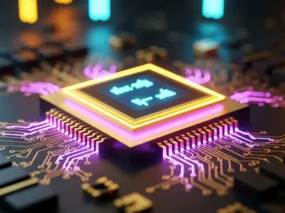
Wafer-scale processors have emerged as a direct response to the limitations of conventional graphics processing units in managing the escalating needs of AI systems. Unlike GPUs, which were initially designed for gaming and later adapted for deep learning, these massive chips integrate hundreds of thousands of cores and vast on-chip memory into a single piece of silicon. This design eliminates the need for data to travel across multiple chips via external networks, a process that often slows down computation and increases energy use. The result is a specialized hardware solution tailored for the intense demands of modern AI applications, particularly large language models that power everything from chatbots to scientific simulations.
The significance of this technology lies in its ability to address a critical pain point: latency. As AI models grow, the time it takes to process and respond to queries becomes a limiting factor, especially in time-sensitive scenarios. By consolidating resources on a single wafer, this innovation offers a paradigm shift, moving away from the sprawling GPU clusters that dominate current infrastructure. It represents a bold step toward efficiency, setting the stage for a deeper examination of how these processors perform in practical settings and what they mean for the future of computing.
Diving into Features and Performance
Unmatched Memory and Processing Capacity
At the heart of wafer-scale processors is their extraordinary capacity for on-chip memory and processing power. These chips, roughly five times larger than traditional GPUs, house an immense number of individual cores, allowing for parallel computation on a scale previously unimaginable. This architecture ensures that data remains localized, slashing the delays associated with transferring information across separate chips in a GPU cluster. For AI systems that rely on rapid access to vast datasets, this feature translates into a dramatic boost in efficiency and speed.
Beyond raw power, the design minimizes energy waste, a growing concern as AI workloads scale. Traditional setups often expend significant resources on inter-chip communication, whereas wafer-scale processors streamline operations within a unified structure. This efficiency is particularly vital for tasks involving large language models, where the ability to handle massive computations without bottlenecks can redefine performance standards in the industry.
Cutting-Edge Low-Latency Architecture
Another standout feature is the ultra-low latency achieved through localized processing. By reducing data movement across distant components, wafer-scale processors cut down on the delays that plague multi-chip systems. This advantage is crucial for real-time AI applications, such as fraud detection in financial transactions or instant responses in conversational AI tools. The ability to process information with minimal wait times enhances responsiveness, making these chips ideal for scenarios where every millisecond counts.
Performance metrics further highlight this edge. Compared to GPU clusters, wafer-scale processors have demonstrated up to a tenfold reduction in latency for specific tasks, alongside notable improvements in energy use. These characteristics position them as a compelling option for industries that prioritize speed and reliability, offering a glimpse into how hardware can evolve to meet the urgent demands of modern AI-driven solutions.
Industry Trends and Innovations
Recent advancements in wafer-scale technology underscore a broader movement toward specialized AI hardware. A notable development is the introduction of tailored software solutions like WaferLLM, born from collaborations between academic institutions and tech giants. This software optimizes large language model performance by reorganizing data flow to prioritize local core communication, significantly enhancing speed—up to 100 times faster text generation compared to earlier implementations—and reducing latency compared to GPU setups.
Beyond specific innovations, the industry is witnessing a shift toward hardware-software co-design. This approach recognizes that raw computational power alone cannot sustain AI growth; instead, integrated systems that align hardware capabilities with software optimization are becoming essential. Additionally, a focus on energy efficiency and cost reduction is shaping research and development, as stakeholders seek sustainable alternatives to the resource-intensive GPU clusters that currently dominate the landscape.
These trends point to a future where AI infrastructure moves beyond simply scaling up existing solutions. Wafer-scale processors are carving out a niche by addressing specific pain points, complementing rather than replacing GPUs. As this technology matures, its influence on system design and operational priorities is expected to grow, potentially redefining how computational challenges are approached over the coming years.
Real-World Impact and Applications
The practical deployment of wafer-scale processors is already making waves across diverse sectors. In healthcare, these chips accelerate drug discovery by enabling AI to evaluate countless molecular combinations at unprecedented speeds, shortening research timelines. Meanwhile, in finance, their low-latency processing enhances fraud detection systems, allowing for real-time analysis of massive transaction datasets to flag suspicious activities before damage occurs.
Public-sector applications are equally promising. Policy analytics, for instance, benefit from rapid data processing to model complex societal trends, aiding in informed decision-making. These use cases illustrate how the efficiency and speed of wafer-scale technology translate into tangible outcomes, improving both operational capabilities and end-user experiences in critical areas.
Specific implementations further showcase this impact. Organizations leveraging these processors report significant advancements in handling large-scale AI tasks, from scientific breakthroughs to enhanced customer service tools. Such examples underline the potential for this hardware to drive progress in fields where computational bottlenecks once limited innovation, paving the way for broader adoption as the technology evolves.
Navigating Challenges and Constraints
Despite their promise, wafer-scale processors face notable hurdles that temper their immediate impact. One key issue is the limited memory per core, which necessitates frequent data sharing within the chip. While local data access is swift, retrieving information from distant parts of the wafer can introduce delays, causing cores to idle and reducing overall efficiency. Efforts like WaferLLM aim to mitigate this by optimizing data distribution, but solutions remain in the early stages of refinement.
Software development presents another significant barrier. Unlike GPUs, which benefit from decades of established programming frameworks, wafer-scale technology requires entirely new approaches. Crafting compatible software demands substantial resources and expertise, slowing widespread adoption. This gap highlights the need for sustained collaboration between hardware engineers and software developers to build a robust ecosystem that can support diverse applications.
Additionally, the physical constraints of such large chips pose manufacturing and scalability challenges. Ensuring consistent performance across an expansive silicon surface is no small feat, and current limitations suggest that these processors may remain specialized tools rather than universal solutions. Addressing these obstacles will be critical to unlocking their full potential in the competitive AI hardware landscape.
Looking Ahead to Future Possibilities
The trajectory of wafer-scale processors points to a specialized yet impactful role in AI infrastructure. Their ability to handle high-demand, latency-sensitive workloads positions them as a valuable asset for specific use cases, even as GPUs retain dominance in general-purpose computing. Looking forward, potential integration with GPU architectures could lead to hybrid systems that combine the strengths of both technologies, offering flexibility alongside efficiency.
Sustainability remains a key consideration for future development. As AI models continue to expand, the energy and cost savings offered by wafer-scale designs could drive significant shifts in how computational resources are allocated. Advances in co-design, blending hardware innovation with software optimization, are likely to yield further breakthroughs, enhancing scalability and performance over the next few years, from 2025 onward.
Exploration of new applications will also shape this technology’s evolution. As industries recognize the benefits of ultra-fast processing, demand for tailored solutions may spur investment in overcoming current limitations. The long-term vision includes a landscape where wafer-scale processors contribute to a more balanced and resource-conscious AI ecosystem, addressing both technical and environmental challenges through thoughtful innovation.
Reflecting on the Journey and Next Steps
Looking back, the emergence of wafer-scale processors marked a pivotal moment in addressing the computational bottlenecks that hindered AI progress. Their ability to slash latency, boost speed, and enhance energy efficiency stood out as a game-changer for specialized workloads, even as challenges in software and on-chip communication persisted. The technology proved its worth in real-world scenarios, from healthcare to finance, demonstrating that hardware innovation could indeed keep pace with the demands of modern AI.
Moving forward, the focus shifts to actionable strategies for broader adoption. Investment in software ecosystems becomes a priority, with an emphasis on creating tools that can simplify programming for these unique chips. Collaborative efforts between academia and industry are encouraged to tackle technical constraints, while exploration of hybrid systems offers a pathway to integrate wafer-scale benefits into existing infrastructures. These steps promise to solidify the role of this technology in shaping a more efficient and responsive future for AI-driven solutions.