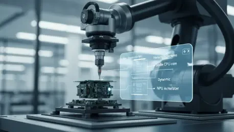
For decades, the microcontroller unit industry operated as a bastion of stability and incremental evolution, where the fundamental architecture—comprising a reliable CPU core, Flash memory, and SRAM—was perfectly honed for its mission in industrial control, automotive electronics, and countless terminal devices. This established paradigm, which prioritized deterministic real-time performance and ultra-low power consumption above all else, remained largely unchallenged because it flawlessly met the demands of its target applications. However, this long-standing equilibrium has been irrevocably shattered by the burgeoning demands of artificial intelligence at the edge. The need to execute sophisticated AI workloads directly on small, power-constrained devices is catalyzing a revolutionary shift in MCU design, pushing the industry away from simple performance upgrades and toward a new class of microcontroller architecturally reimagined from the ground up. A clear consensus has now emerged among the industry’s leading players that the future of the MCU lies in a heterogeneous architecture, one that intelligently fuses traditional control functions with dedicated AI capabilities to enable a new generation of smart devices without sacrificing the foundational virtues that define embedded systems.
The NPU Imperative for Control and Efficiency
The primary driver behind this architectural revolution is the strategic integration of a Neural Processing Unit (NPU), whose most critical role in an embedded context is to achieve what is known as “computing power isolation.” In traditional MCU designs, tasking the main CPU with both its primary real-time control duties and the computationally intensive demands of AI inference creates a fundamental conflict. AI tasks are resource-heavy and can introduce unpredictable latency, which threatens to delay crucial control interrupts and destroy the system’s time determinacy—a non-negotiable requirement in safety-critical applications like automotive braking systems or industrial robotics. The NPU functions as a dedicated, independent hardware accelerator that offloads all AI-related computations, from sensor data analysis to image recognition. This architectural segregation is the key to enabling advanced intelligence without compromising the bedrock reliability of embedded systems, as it allows the main CPU to focus exclusively on its core mission of deterministic, microsecond-level control while the NPU handles complex inference tasks in parallel. This separation ensures that the addition of AI enhances, rather than undermines, the system’s core function.
Beyond preserving real-time determinism, a second critical driver for NPU integration is the rigorous management of power and thermal envelopes. Embedded systems, particularly battery-powered IoT devices and automotive components operating in harsh environments, are governed by extremely tight power budgets. A dedicated NPU, constructed with fixed-function hardware like MAC arrays and systolic arrays, offers a highly efficient and, crucially, a predictable power consumption profile for executing AI workloads. This predictability is vital for system designers who must manage thermal output and guarantee long battery life. In contrast, running AI models on a general-purpose CPU results in far less efficient processing and leads to unpredictable power spikes that are unacceptable in these constrained environments. Therefore, the embedded NPU is best understood not as an “engine” designed to maximize raw performance but as a “shock absorber.” Its primary function is to absorb the computational impact of AI, thereby protecting the stability and responsiveness of the main real-time control system. This is why the computing power of these NPUs is deliberately restrained, typically ranging from tens to hundreds of Giga Operations Per Second (GOPS), a mere fraction of the multi-TOPS capabilities seen in mobile processors or cloud GPUs. This restraint is a conscious design choice, as excessive computing power would lead to a larger chip area, higher costs, and increased power consumption—all antithetical to the core principles of embedded system design.
A Unified Goal with Diverse Strategies
While major MCU manufacturers agree on the necessity of this new architecture, their implementation strategies reveal distinct philosophies tailored to their respective market strengths. Texas Instruments, for instance, is leveraging its historical dominance in real-time control by deeply embedding NPU capabilities into its existing ecosystem, creating a “control + AI” integrated solution primarily for industrial and automotive safety scenarios. Its TMS320F28P55x series, the industry’s first real-time MCU with an NPU, exemplifies this by pairing a classic C28x DSP core with a CNN-optimized NPU. This design achieves perfect computing power isolation, allowing the NPU to be used for tasks like arc fault monitoring and motor fault diagnosis, where it improves detection accuracy to over 99% and reduces latency by a factor of 5-10, all while the main CPU remains dedicated to its microsecond-level deterministic control tasks. TI supports this hardware with its Edge AI Studio toolchain and ensures its products meet stringent functional safety standards like ISO 26262, reinforcing its commitment to high-reliability applications where failure is not an option.
In contrast, Infineon has adopted a more lightweight and broad-market approach, strategically leveraging the mature Arm ecosystem to lower the development barrier for edge AI and rapidly cover a wide array of applications, from consumer IoT to industrial Human-Machine Interfaces (HMIs). Their PSOC Edge E8x series demonstrates a tiered strategy, using a combination of Arm Cortex-M cores (M33/M55) and AI accelerators like Arm’s Ethos-U55 micro-NPU. By utilizing standard Arm components, Infineon ensures extremely low power consumption—the Ethos-U55 operates at the milliwatt level—and benefits from a vast existing software ecosystem. Their competitiveness is further bolstered by their ModusToolbox development platform and the integration of tools like Imagimob Studio, which provides customers with a complete, end-to-end development path from data collection to model deployment, making sophisticated edge AI accessible to a broader range of developers.
NXP’s strategy is centered on providing a highly flexible and scalable solution that can adapt to a diverse range of neural network models, targeting applications like industrial robotics and smart automotive systems. To achieve this, NXP developed its own eIQ Neutron NPU, which features a scalable architecture that allows customers to precisely tailor the computing power to their specific needs. A key differentiator for NXP is its unified eIQ AI software toolkit, which supports mainstream frameworks like TensorFlow Lite and PyTorch. This enables customers to “bring their own model” for localized processing, a critical feature for enhancing data privacy and reducing latency. The company’s emphasis is on delivering a full-stack solution where a powerful, flexible hardware platform is supported by a comprehensive and accessible software ecosystem, empowering engineers to deploy custom AI solutions with greater ease and control.
Meanwhile, STMicroelectronics is targeting the high-performance end of the edge AI market, particularly industrial vision and advanced consumer electronics, where processing power is paramount. Their strategy involves pairing a high-performance core with a powerful, self-developed NPU to break the traditional performance limits of MCUs. The STM32N6 series is a prime example of this approach, featuring an 800MHz Arm Cortex-M55 core and their Neural-ART Accelerator NPU running at up to 1GHz, delivering an impressive 600 GOPS of AI performance. To cater specifically to vision applications, the chip integrates a complete processing pipeline, including a MIPI CSI-2 camera interface, an Image Signal Processor (ISP), and an ##64 hardware encoder. This allows it to handle high-resolution image processing and complex tasks like real-time object detection directly on the MCU, supported by ample on-chip RAM and high-speed external memory interfaces, effectively turning the microcontroller into a compact vision system.
Renesas has built its core strategy on the twin pillars of a heterogeneous computing architecture and robust, multi-layered security, focusing intently on high-reliability edge AIoT scenarios like smart homes and industrial predictive maintenance. Their products, such as the RA8P1 MCU, utilize a multi-core architecture (e.g., Cortex-M85 combined with a Cortex-M33) alongside an Arm Ethos-U55 NPU. This heterogeneous approach is deeply integrated with a sophisticated security engine that supports Arm TrustZone, a hardware root of trust, and even forward-looking solutions like post-quantum cryptography (PQC). Renesas’s goal is to ensure that as edge devices become more intelligent and connected, they are also fortified against escalating network security threats. By making security an integral part of the AI implementation rather than just an add-on, Renesas is positioning its products for a future where both intelligence and trust are indispensable.
Beyond Processing and the Memory Bottleneck
The integration of NPUs is only one half of this architectural revolution; the other critical transformation is occurring within the memory subsystem. The dynamic nature of AI workloads exposes the fundamental limitations of the traditional Flash memory that has long been the cornerstone of MCUs, creating a series of dilemmas that demand a new approach to data storage. The first of these is the “Model Lifecycle Dilemma.” Edge AI models are not static; they require frequent Over-the-Air (OTA) updates for continuous improvement and adaptation to new data. However, traditional Flash memory has a limited endurance, typically rated for only a few thousand to tens of thousands of erase/write cycles. The constant stream of model updates necessary to keep an AI device effective would rapidly degrade the Flash, potentially causing the chip to fail long before the end of the product’s intended lifespan. This limitation makes conventional Flash untenable for the dynamic lifecycle of modern AI applications.
This challenge is compounded by the “Edge Learning Dilemma,” which arises from the emerging field of on-device model training and adjustment. This capability, which allows a device to learn from its local environment, is incompatible with the traditional Flash/SRAM architecture. Model parameters stored in Flash cannot be efficiently modified in real-time due to slow write speeds and the block-based nature of erase operations. While SRAM allows for the necessary fast read/write access, its capacity is typically very limited to a few megabytes, and it is volatile, meaning all data is lost upon power-off. This makes SRAM unsuitable for persistently storing adjusted model parameters, effectively preventing devices from achieving true, on-device learning. This architectural bottleneck inhibits the development of more autonomous and adaptive edge systems, which represent the next frontier of AI.
Finally, the “Startup Performance Dilemma” highlights another critical shortcoming of Flash memory in an AI-enabled world. Many embedded applications, especially in industrial and automotive settings, require “instant-on” capabilities where the system must be fully operational immediately upon power-up. The inherent read latency and “warm-up” time associated with fetching a potentially large AI model and its associated firmware from Flash memory can introduce unacceptable delays during system startup. This latency can impact overall system efficiency, compromise safety in time-critical applications, and degrade the user experience. These three dilemmas collectively illustrate that Flash memory, while excellent for traditional firmware storage, is ill-suited for the dynamic and performance-sensitive demands of AI. This has created an industry-wide imperative to move toward new types of non-volatile memory that offer a combination of high endurance, fast write speeds, and low latency, thereby providing the robust memory foundation required to fully unlock the potential of AI-enabled MCUs.
Charting the New Embedded Frontier
In navigating this profound architectural shift, the embedded industry successfully moved beyond decades of incrementalism. The challenge presented by edge AI was met not with a simple increase in clock speeds, but with a fundamental rethinking of the microcontroller itself. The strategic integration of dedicated Neural Processing Units became the cornerstone of this new paradigm, providing the necessary computational offload to preserve the sanctity of real-time control loops. Simultaneously, the industry confronted the deep-seated limitations of its memory subsystems, recognizing that traditional Flash memory was a bottleneck to the dynamic lifecycle of AI models. This dual focus on both processing and memory led to the rise of truly heterogeneous systems, where performance, power efficiency, security, and data persistence were treated as interconnected design pillars. The solutions that emerged from this period established a new blueprint for embedded design, one that prepared the industry for a future of increasingly autonomous, intelligent, and secure devices at the farthest reaches of the network.


